Gurtej Sandhu: The Quiet Innovator Who Surpassed Edison and Revolutionized Semiconductor Technology
Introduction
In an era dominated by flashy tech moguls and celebrity inventors, Gurtej Singh Sandhu stands as a beacon of understated brilliance. Born in 1960 to Indian immigrant parents in London, Sandhu has quietly amassed over 1,382 U.S. utility patents, securing his place as the seventh most prolific inventor in history—surpassing Thomas Edison's 1,093 patents. As a Senior Fellow and Vice President at Micron Technology in Boise, Idaho, Sandhu's work in semiconductor fabrication has underpinned the digital revolution, enabling the miniaturization of memory chips that power everything from smartphones to cloud servers. His innovations have extended Moore's Law, the principle predicting the doubling of transistors on microchips approximately every two years, ensuring affordable, high-performance electronics for billions.
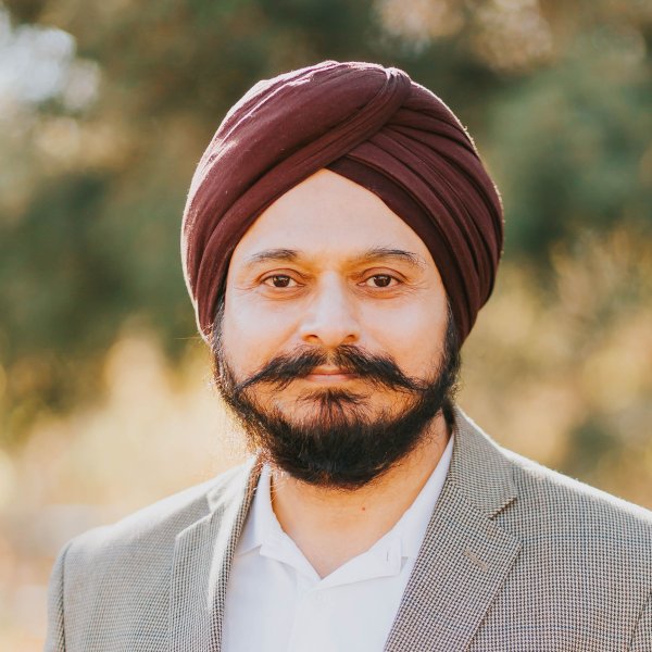
Yet, Sandhu remains remarkably low-profile. A devout Sikh who wears a turban and maintains a beard, he embodies humility and perseverance—values rooted in his faith and upbringing. As of September 2025, recent media coverage, including articles from Hindustan Times and News18, has spotlighted his ties to Guru Nanak Dev University (GNDU) in Amritsar, Punjab, celebrating him as a national pride.
Early Life and Family Background
Gurtej Sandhu's journey began on October 24, 1960, in London, England, where his Sikh parents had migrated seeking better opportunities. At age three, the family returned to India, settling in Punjab, a region rich in cultural and agricultural heritage but marked by economic challenges. Sandhu grew up in a modest household, surrounded by the vibrant Sikh community, which emphasized education, discipline, and service (seva). His parents, both chemistry graduates, instilled a passion for science despite financial constraints. As Darpan Magazine (2022) notes, "Dr. Sandhu’s passion for invention and research is rooted in his upbringing... As a child, he was quiet and shy, yet deeply introspective. He recalls asking all kinds of adult questions about the origin of the universe and the meaning of life and death."
This introspective nature set Sandhu apart. In Punjab, he pondered existential queries amid a supportive family network—uncles in chemical engineering further fueled his curiosity. Recent 2025 reports from Hindustan Times and Tribune India highlight his connection to Amritsar, portraying him as a GNDU alumnus whose early education there laid foundational stones. Though details on his primary schooling are sparse, sources like SikhiWiki (2024) suggest exposure to Sikh principles of equality and hard work shaped his resilience. Sandhu has spoken of facing stereotypes as a turbaned Sikh, yet he views it positively: "Being memorable in professional settings" (Darpan Magazine, 2022).
His family's emphasis on learning amid adversity mirrors the broader Sikh diaspora experience. Immigrants like his parents balanced cultural roots with global aspirations, teaching Sandhu tenacity. No scandals or setbacks define this period; instead, it reflects quiet determination. By his teens, Sandhu's interest in electronics emerged, inspired by India's growing tech scene. This foundation propelled him toward higher education, where his innate problem-solving skills would flourish.
Expanding on his cultural ties, 2025 Instagram reels and Facebook posts (e.g., from August 30, 2025) celebrate Sandhu as a "58-year-old Indian-origin Sikh scientist" (noting his age inaccurately, as he turns 65 in 2025), emphasizing how his heritage informs his ethical approach to innovation. In interviews, like one on YouTube's "The Silent Genius Who Surpassed Thomas Edison" (August 7, 2025), Sandhu credits his parents for encouraging curiosity without pressure, fostering a mindset that views failure as iterative learning.
Education and Immigration to the United States
Sandhu's academic path solidified his destiny in technology. He pursued electrical engineering at the prestigious Indian Institute of Technology (IIT) Delhi, earning a degree in the 1980s—sources vary between B.Tech and M.Tech, but Wikipedia confirms it as foundational in chip fabrication. At IIT, he discovered semiconductor physics, blending electrical engineering with materials science. This era in India, post-economic liberalization, sparked his interest in integrated circuits, though limited resources pushed him abroad.
In the late 1980s, Sandhu immigrated to the U.S. for a Ph.D. in Physics at the University of North Carolina at Chapel Hill, completed in 1990. His dissertation explored semiconductor materials, aligning with the booming tech industry. As Brain Gain Magazine (2019) quotes him: "My skills were in high demand" after graduation, leading to multiple offers. Discrepancies in sources—SikhiWiki claims Electrical Engineering, but IEEE specifies Physics—underscore his interdisciplinary expertise.
Immigration posed challenges: cultural adjustment, visa hurdles, and bias against visible minorities. Yet, Sandhu chose Boise over Silicon Valley for its family-oriented environment and Micron's potential. This move, detailed in Spokesman-Review (2018), marked his integration into America's innovation ecosystem. Recent 2025 coverage from DNA India (August 13, 2025) lauds him as an "Indian-origin scientist who surpassed Thomas Edison," highlighting his journey from Punjab to global prominence.
His education emphasized fundamentals like thin-film deposition, preparing him for real-world R&D. In a TEDxBoise talk (2019), Sandhu reflects: "Innovation transforms our planet—for good," stressing curiosity's role. Mentors at UNC honed his skills, while IIT's rigor built resilience. Today, he mentors at Boise State University, closing the loop on educational giving back.
Career Trajectory at Micron Technology
Joining Micron in 1990 as an entry-level engineer, Sandhu transformed a mid-tier company into a semiconductor giant. Micron, then ranked 18th globally, now boasts $20+ billion in revenue, thanks partly to his leadership. He rose to Senior Fellow and Director of Advanced Technology Developments in the early 2000s, then Vice President, overseeing R&D for DRAM and NAND memory.
His career milestones include:- 1990s: Pioneering thin-film processes.- 2000s: Integrating atomic layer deposition for 90-nm DRAM.- 2010s: Advancing NAND via pitch-doubling.- 2020s: Exploring AI and DNA storage, as in his 2024 YouTube talk "Science in the Age of Experience."
Sandhu's loyalty is notable; despite offers, he stayed, saying in Brain Gain Magazine (2019): "Sitting in Boise, Idaho, and working for Micron, and everybody in the world is using your patent... that's the reward." At Micron, he leads global teams, fostering collaboration. 2025 news from Beyond the Punchlines (August 2, 2025) notes his 1,382 patents, impacting 90% of electronics.
In a YouTube interview "Micron engineer has more patents than Thomas Edison" (2018), Sandhu describes invention as "problem-solving for work." His role now includes strategic tech pathfinding, using physics modeling and AI for future chips.
Career Milestones
1990 - Joins Micron: Begins process engineering as entry-level engineer.
Early 2000s - Senior Fellow: Promoted to Senior Fellow, leads advanced technology developments.
2010s - Vice President: Oversees global R&D for memory scaling.
2025 - Current Focus: AI-driven innovations and emerging memory technologies.
Key Inventions and Technological Impact
Sandhu's patents focus on sustaining Moore's Law through semiconductor scaling. Wikipedia lists key ones:- Titanium Coating Method (1990s): Prevents oxidation; now industry-standard. Sandhu understated it: "Suddenly it clicks" (Kiplinger, 2008).- Atomic Layer Deposition (ALD) for High-κ Films (2000s): Enabled 90-nm DRAM scaling.- Pitch-Doubling Process (2000s): Produced first 3X-nm NAND, using lithography: ( \text{Pitch} = \frac{\text{Line Width} + \text{Space}}{2} ), doubling density.- Large-Area Straight-Wall Capacitors: Extended 1T1C DRAM.- CVD Ti/TiN Process: Barrier layers for chips.- Recent: DNA-based storage, per 2024 YouTube talk.
These underpin modern devices. As IEEE (2018) states: "Pioneering achievements in patterning and materials integration." Darpan Magazine (2022) quotes: "My main passion is to solve complex problems... The patents are simply a byproduct."
2025 updates from Hindustan Times (August 2, 2025) confirm 1,382 patents, with potential growth. His work addresses physical limits, like quantum effects, via innovative materials.
Key Inventions and Their Global Impact
Ti Coating (1990s): Prevents chip ruin; used in most memory makers.
ALD High-κ (2000s): Scaled DRAM for smartphones.
Pitch-Doubling (2000s): Boosted NAND storage density.
DNA Storage (2020s): Explores biological alternatives to silicon.
Awards, Recognition, and Societal Contributions
Sandhu's accolades include the 2018 IEEE Andrew S. Grove Award for "pioneering achievements" in memory scaling, with a medal and honorarium. At Darpan's 2022 Awards, he received a standing ovation as the "seventh most prolific inventor."
He mentors at Boise State for 15+ years, launching its Materials Science Ph.D. and securing funding. Brain Gain Magazine quotes: "I want to do more to help make young students... excited about science." Ties to GNDU include support, per Tribune India (2025).
In TEDx (2019), he advocates innovation for good. As a Sikh, he promotes diversity in STEM, facing but overcoming biases.
Personal Life, Philosophy, and Legacy
At 64, Sandhu lives privately in Boise, rooted in Sikh values of humility. He says: "Tenacity, curiosity, and attention to detail" drive him (Darpan, 2022). In YouTube's "Innovation Mindset at Micron" (2021), he encourages out-of-box thinking.
His legacy: Democratizing tech, inspiring immigrants. 2025 YouTube video "Meet Sikh Inventor Gurtej Sandhu" (2019 update) calls him the "world's 7th best inventor."
Conclusion
Gurtej Sandhu's life exemplifies how quiet perseverance can reshape the world. From Punjab's fields to Micron's labs, his 1,382 patents have fueled the digital age, surpassing Edison while honoring his roots. As 2025 news celebrates his GNDU ties, Sandhu reminds us: Innovation serves humanity. His story urges future generations to blend heritage with bold ideas, ensuring technology's inclusive future.